


Fine line technology
The driving forces in electrical engineering today are higher integration and minimal dimensions. The chip industry is continuously setting new standards and dictating the pace in the area of fine line technology.
This trend is driven by the desire for ever lower power consumption and the integration of increasing amounts of logic into the circuit carriers. Nowadays, fine line technology can be found in many everyday products, such as sensors, actuators and components in control technology. Radar sensors support us unnoticeably in everyday life by detecting traffic obstacles or measuring industrial flow rates.
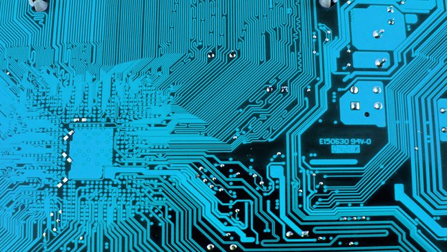
The highest quality standards in manufacturing processes and tight tolerances in conductive pattern production are essential requirements for PCBs featuring fine line technology that connect highly integrated chips with peripheral electronics.
VARIOPPRINT has recognised this trend and is making every effort to keep pace with the miniaturisation in the chip industry. Recent investments in laser exposure systems, electroplating and registration technology support us in this continuous improvement process.
Current status VARIOPRINT Standard:
- Line / space 75 µm / 75 µm
- Standard: Via / pad 75 µm / 300 µm
- Special: Line / space 50 µm / 50 µm
- Special: Via / pad 40 µm / 200 µm
- Thinnest base copper: 9-5 µm
- Thinnest base material: 25 µm
In construction at VARIOPRINT
- Line / space 25 µm / 25 µm
- Standard processing of copper thicknesses <10 µm