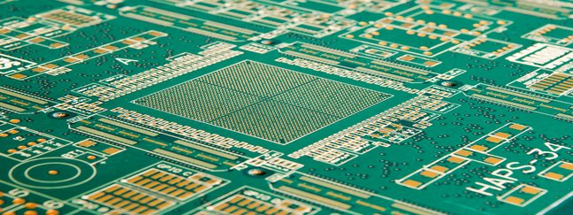
Multilayer / HDI PCBs
Thinking of tomorrow, today -
Microvia technology from VARIOPRINT
Optimal, fully-automated processing, accurate registration processes and reliable through-plating technologies guarantee the supreme quality and reliability of our products. Rising frequencies require impedance-controlled circuits and increasingly higher signal integrity. Multilayer circuits also allow the separation of analog and digital parts on a circuit board.
We started manufacturing multilayer circuit boards as early as 1985. However, today's products are very different from the pioneers of that time. The multilayer circuits of today are characterised by ultra-thin cores of 50 µm thickness, and micro-structures that nonetheless feature a higher numbers of layers.
When developing and designing new solutions, we are driven by the principle of smaller, lighter, thinner and yet with an increasing number of functions.
The higher packaging densities of components require new layout structures. Integrated blind and/or buried vias, copper-filled blind vias and plugged vias are state of the art and manufactured by VARIOPRINT with maximum process stability. The latest laser systems for drilling and contouring and the most advanced vertical electroplating facility in Europe guarantee the highest possible product quality.
Performance range
Design and technology Blind vias, buried vias, μVias with and without copper fill and plugged vias with/without overplating.
|
| Dimension and formats Thickness 0.2 mm to 4.8 mm Format up to 569x490 mm Panel formats used 460x610 mm und 530x610 mm |
Solder resists and additional prints Additional prints, such as legend print, peelable mask and carbon print
|
| Conductive pattern structuring Copper cladding from 18 μm to 210 μm Conductor widths and spacings Standard: 75 µm / 100 µm Special: 50 µm / 50 µm possible |
Mechanical machining Annular rings |
Materials Standard glass fabric type 106/1080/2116 and 7628, additional types according to requirement and design |
| End surfaces Various chemical and galvanic gold surfaces and chemical tin and silver surfaces, as well as pure organic protective coatings |
| Electroplating and copper plating Aspect ratio up to 1:12 with 0.15 mm drill diameter 1:15 with 0.3 mm drill diameter Copper in vias in accordance with IPC II, IPC III or customer specific
|


